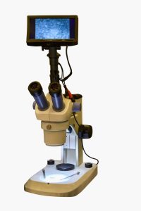
The electron microscope is a type of microscope that uses a beam of electrons to create an image of the specimen. It is capable of much higher magnifications and has a greater resolving power than a light microscope, allowing it to see much smaller objects in finer detail.
All electron microscopes use electromagnetic and/or electrostatic lenses to control the path of electrons. Glass lenses, used in light microscopes, have  no effect on the electron beam. The basic design of an electromagnetic lens is a solenoid (a coil of wire around the outside of a tube) through which one can pass a current, thereby inducing an electromagnetic field. The electron beam passes through the center of the solenoids on its way down the column of the electron microscope towards the sample. Electrons are very sensitive to magnetic fields and can therefore be controlled by changing the current through the lenses.
There are two main types of electron microscope – the transmission EM (TEM) and the scanning EM (SEM). The transmission electron microscope is used to view thin specimens (tissue sections, molecules, etc) through which electrons can pass generating a projection image. The TEM is analogous in many ways to the conventional (compound) light microscope. TEM is used, among other things, to image the interior of cells (in thin sections), the structure of protein molecules (contrasted by metal shadowing), the organization of molecules in viruses and cytoskeletal filaments (prepared by the negative staining technique), and the arrangement of protein molecules in cell membranes (by freeze-fracture).
Recently, a record-breaking electron microscope has been developed that can produce images at a higher resolution than conventional approaches have been able to achieve, making it suitable for studying fragile materials that can be damaged by electron beams.
This produced the highest-magnification image ever obtained using a transmission electron microscope. The image reveals the atoms in a two-dimensional self-supporting sheet of a semiconductor, and has a resolution of 0.39 angstrom for comparison, most atoms are about 2–4 Å in diameter. The technique might eventually allow 2D materials to be examined with unprecedented precision, providing insight into this burgeoning class of useful compounds. It might also lead to the development of a method that can image individual atoms in 3D objects.
To obtain higher resolution images requires the use of a precision lens that has been designed and manufactured with precise accuracy and clarity. That is where Universe Optics comes in. Our team of developers, along with our manufacturing department, will work with your specifications to ensure your lens is of the highest quality.
This development could ultimately provide a way of precisely imagine the 3D bonding of every single atom in a solid volume of matter, while using a minimal flux of damaging electrons. It is also suggested that the next step is to use the process for tomography. The goal would be to solve the exact 3D atomic structures of solids that have no long-range order, such as nanocrystalline materials, glasses and amorphous metals, for which researchers must currently infer structures from averaged bulk measurements.