
UV lenses are transforming industries worldwide thanks to a significant boost in technology. One example is the semiconductor industry making the most out of thermal imaging lenses.
Semiconductor Chip Production
Semiconductor chips are a primary component in computers, cell phones, cars, and appliances. Manufacturers use photolithography, which involves shining light through a mask onto a wafer coated with a light-sensitive material to create them. This exposure to light changes the material’s properties, allowing the etching of patterns onto the surface of the wafer.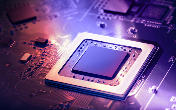
UV Lens Types Used In Semiconductor Production
UV lenses are used in photolithography to focus the light onto the wafer. They utilize materials that allow UV light to pass through, such as quartz or calcium fluoride. There are different types of UV lenses, including refractive and Fresnel lenses.
Refractive lenses derive from a single material, such as quartz. They work by bending the light as it passes through the lens. Fresnel lenses are the product of a series of curved surfaces. They work by redirecting the light and focusing it onto the wafer.
UV lenses are standard in both projection and scanning photolithography systems. In projection systems, the mask is in the path of the UV light. The light passes through it and focuses onto the wafer by the lens.
UV Lenses Use Materials Differently
UV lenses utilize various materials, including quartz, calcium fluoride, and magnesium. Each material has unique properties making it suitable for different applications. For example, quartz lenses are used in high-end projection systems because they have a high index of refraction, which allows them to focus the light onto the wafer with a higher degree of accuracy.
Calcium Fluoride
Calcium fluoride lenses are used in scanning systems because they have a lower refraction index, making them less likely to cause diffraction artifacts. Finally, magnesium fluoride lenses are used in both projection and scanning systems because they have a high transmission rate, allowing more light to reach the wafer.
The semiconductor industry constantly evolves, and new manufacturing processes are under development. UV lenses play a vital role in these processes, and their use will likely continue to grow.
UV Lenses Excel At Quality Monitoring And Inspection
Semiconductor fabrication requires accuracy. Any mistake can cause a chip to fail, so monitoring for quality is an integral part of the production process. UV lenses are helpful because they can find tiny defects early in production.
Inspecting parts at high speeds reduces manufacturing defects and prevent poor products from shipping.
Traditionally, machine-vision lenses have functioned in the visible spectrum, allowing captured images to represent what humans can see. LEDs are in use in some non-UV applications; however, the resolvable resolution that users can obtain in the visible spectrum has prompted the development of lenses that function in the UV region of the electromagnetic spectrum.
Detailed Resolution Boosts Accuracy
The resolving frequency achievable by such lenses is higher because the wavelength of UV light is shorter than that of visible, allowing more detailed object resolutions to be detected. That boosts their usability in semiconductor manufacturing, empowering companies to check for errors and monitor the production process quickly.
Defect Review Systems Continue To Speed Up
The semiconductor inspection process focuses on shorter-wavelength light, thanks to chips getting smaller. Slimmer chips mean tinier defects requiring even more precise cameras and lenses to detect.
Manufacturers are creating new systems using defect-review imaging, reticle, and wafer inspection tools. The new designs use cameras and optics operating in the 150nm to 300 nm deep-UV.
The trend in using UV technology and UV lenses is following that of semiconductor fabrication. As a result, products are getting smaller and faster, making them available for further advances.
UV lenses are irreplaceable in product inspections. They help eliminate any bottlenecks that might arise from less automated means of checking each unit to ensure error-free. In addition, they keep improving their core functions and will continue to play a crucial role in detecting product quality issues.
More Innovations Are On The Horizon
The trends indicate that UV lenses will become crucial to companies making fabricated chips. Many breakthroughs are happening in extreme UV (EUV) photolithography.
Those advancements continue to unleash new applications that assist semiconductor makers in their core mission. A quick scan of headlines in the past few years will show that EUV technology continues to push through barriers and achieve remarkable speed.
EUV is the most significant technical innovation in three decades and will be instrumental in helping semiconductor manufacturers keep up with rising demand.